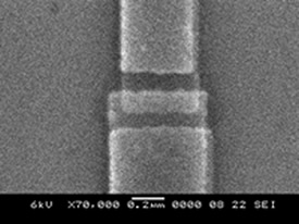
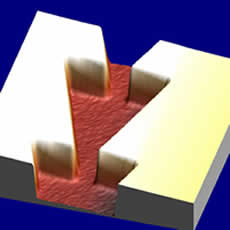
The devices we study involve thin films of superconductors and normal metals deposited with a variety of techniques onto substrates, typically silicon or sapphire. The methods for patterning and depositing the films are similar to techniques in the microelectronics industry. For large-scale features, we use photolithography, where a polymer resist is exposed optically to define a particular pattern. This technique can produce features with linewidths down to the micron scale. To transfer submicron patterns, necessary especially for the small-capacitance tunnel junctions in the quantum coherence experiments and narrow channels in vortex dynamics measurements, we use electron-beam lithography, in which a Scanning Electron Microscope (SEM) is employed to write patterns in a polymer resist. With electron-beam lithography, it is possible to produce feature sizes below 100 nm.
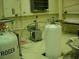
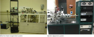
We perform all of our lithography in the state-of-the-art laboratories at the Cornell NanoScale Facility (CNF), about a one-hour drive from Syracuse. We pattern our large-scale features with photolithography and perform various etch processes also at the CNF. We have constructed a dedicated electron-beam evaporation system in our lab here at Syracuse to deposit the aluminum films for the Al-AlOx-Al tunnel junctions. In January 2010 we commisioned a custom sputter system in our lab for depositing a variety of superconducting films, including Nb and a-MoGe. At Syracuse we have access to various optical microscopes, an AFM, and an SEM for sample inspection. For more extensive sample characterization we sometimes make use of the facilities available at the Cornell Center for Materials Research (CCMR).
Cryogenics
Almost all of the measurements in our lab are performed at temperatures close to absolute zero. For any superconducting device, the system must be cooled below the transition temperature of the particular superconductor: 9K for niobium, 6K for a-MoGe, achievable with simple probes immersed in liquid helium-4 — we have constructed several of these for a variety of experiments; 1K for aluminum, achievable with a helium-3 cryostat — we have such a system from Janis Research.
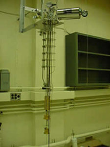
Many of our measurements, in particular, the quantum coherence studies, require even lower temperatures in order to reduce the thermal energy below the other relevant energy scales. These experiments take place in a dilution refrigerator at temperatures below 50 mK. It is a challenge to measure microfabricated circuits at these low temperatures and to ensure that noise and interference from room-temperature electronics do not travel down the electrical leads in the refrigerator and perturb the circuit. Thus, extensive amounts of filtering, attenuation, and shielding are required. At the end of the summer of 2007, we finished building our dilution refrigerator and cooled it for the first time, reaching a base temperature of 30 mK. This system is based on the highly successful design of John Martinis at UC Santa Barbara and provides a large region cooled to the base temperature and has substantial space available for many coaxial lines and electrical filters.